Skip to main content

Key takeaways:
- IoT firmware often hides critical vulnerabilities that attackers can exploit to compromise your IoT products, gain access to sensitive corporate data, and even steal personal information from your customers.
- Reverse engineering is one of the most effective methods for uncovering these hidden risks, as it allows security experts to analyze the actual firmware code, identify insecure implementations, and detect vulnerabilities that standard testing often overlooks.
- Understanding device architecture is essential for effective firmware analysis, and a mix of techniques provides the best security insights.
- Outsourcing firmware reverse engineering to experienced specialists accelerates results and reduces business risk.
In the first five months of 2024, attacks on IoT endpoints grew by 107% year over year. Meanwhile, breaches involving IoT endpoints often cost affected businesses between $5 million and $10 million per incident. Alarmingly, one in three data breaches now involves an IoT device. IoT devices have become powerful entry points in cyber attacks — and for IoT devices manufacturers, these numbers translate into strategic risk.
Securing IoT firmware is no longer optional if you want both product integrity and enterprise safety. In this article, our experts walk you through a real-world example of firmware reverse engineering using a smart air purifier, showing how analyzing architectural components reveals hidden vulnerabilities.
This article will be useful for CTOs, CISOs, product managers, and technical executives who oversee IoT products and seek to proactively fortify their systems by embedding firmware-level security assessments into development and quality assurance processes.
Contents:
- Why is it important to identify firmware vulnerabilities?
- What are the main steps in reverse engineering IoT firmware?
- Best techniques for reverse engineering IoT firmware
- How to reverse engineer IoT firmware the right way: A practical example from Apriorit engineers
- How Apriorit can help with reverse engineering IoT firmware
- Conclusion
Why is it important to identify firmware vulnerabilities?
IoT firmware contains the core business logic of a device and often contains critical intellectual property. Compromising firmware can provide attackers with access to communication mechanisms, user applications, management functions, storage, and even other parts of the ecosystem. For businesses, this means exposure of sensitive corporate data and customer information, and it opens the door to costly breaches.
After identifying vulnerabilities in firmware, your business can:
- Detect and remove hardcoded credentials before attackers exploit them to brute-force access.
- Prevent buffer overflows that could allow malicious actors to execute arbitrary code and take control of devices.
- Find insecure communication protocols and replace them with secure alternatives to block interception and man-in-the-middle attacks.
- Eliminate hidden backdoors that could otherwise give attackers unauthorized control over your IoT solutions.
By combining architectural knowledge with vulnerability analysis, reverse engineers can uncover weaknesses that automated tools might miss. As a result, your business can strengthen product security, protect sensitive customer and corporate data, and reduce the risk of costly breaches or compliance violations.
Let’s take a look at how Apriorit experts recommend reverse engineering IoT firmware.
Want to enhance your IoT project’s security?
Hire professional reverse engineers and IoT developers from Apriorit to deliver a reliable and protected solution.
What are the main steps in reverse engineering IoT firmware?
Every project is unique. However, most IoT firmware reverse engineering efforts follow a common workflow that helps engineers move from raw firmware to actionable insights:
- Acquire the firmware. Extract the firmware from the device (via UART/JTAG, SPI flash dump, or official update files).
- Perform an initial inspection. Analyze the file structure and metadata to identify architecture, compression, and encryption methods.
- Unpack and reconstruct. Break down the firmware image into its components, such as bootloaders, file systems, and binaries.
- Study the architecture and format. Determine the CPU/microcontroller architecture and understand the firmware’s overall structure.
- Analyze code and data. Review binaries, configuration files, and communication logic for potential vulnerabilities.
- Document findings. Record results, create a clear map of the firmware, and highlight areas of concern for further testing.
With this structured process, your teams can systematically uncover weaknesses and guide mitigation strategies even with limited tooling or an unfamiliar architecture. Now, let’s take a look at the most common techniques for reversing IoT firmware.
Best techniques for reverse engineering IoT firmware
To perform reverse engineering of IoT firmware correctly, it’s best to use a mix of hardware and software analysis. Your team might need to choose different methods based on the device architecture, available tooling, and your research goals. Here are some of the most widely used techniques:
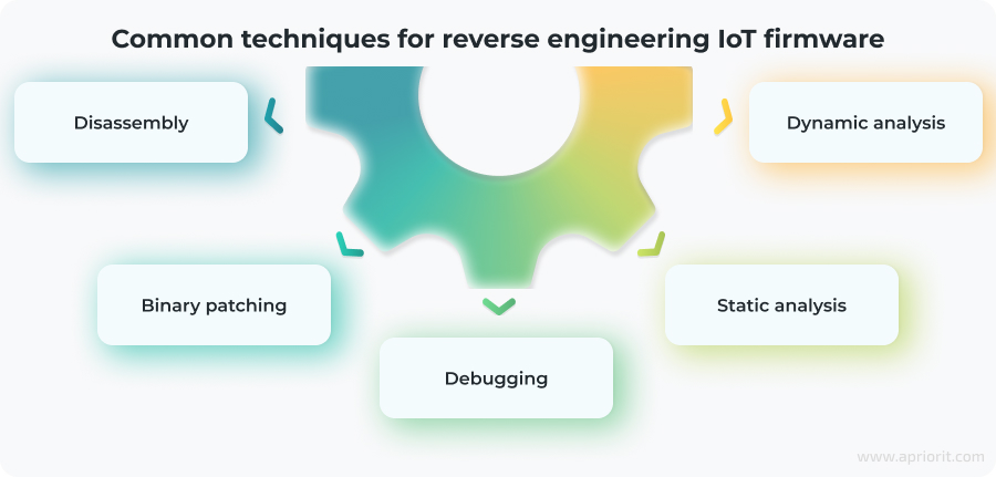
Disassembly
Disassembly translates machine code into human-readable assembly instructions. Common practices include:
- Using tools like IDA Pro, Ghidra, or Radare2 to automate translation
- Identifying function calls, memory access, and control flow
- Comparing different firmware versions to detect changes or hidden functionality
This technique helps researchers understand low-level firmware operations, even when high-level source code isn’t available.
Debugging
Debugging runs firmware in a controlled setting to observe its behavior step by step. Typical steps include:
- Launching firmware with a debugger
- Inspecting memory, stack, and register values during execution
- Connecting to hardware debug interfaces such as JTAG or SWD
- Detecting logic flaws or unsafe memory handling in real time
This approach provides real-time insights into the system state.
Binary patching
Binary patching modifies the firmware binary itself to test or alter device behavior.
Here are some use cases where you can apply binary patching:
- Removing security restrictions for testing
- Patching known vulnerabilities before an official update
- Inserting logging or debugging hooks for deeper analysis
- Testing exploit feasibility without full source code
Static analysis
Static analysis examines the firmware without executing it. Researchers review code structure, configuration files, and libraries to detect vulnerabilities such as hardcoded credentials or unsafe function calls.
Dynamic analysis
Dynamic analysis runs the firmware inside an emulator or on test hardware to monitor its runtime behavior. This helps uncover issues in communication protocols, memory use, and error handling that static analysis might miss. You can include techniques like fuzzing into dynamic analysis for even greater efficiency.
Understanding these techniques can provide you with a strong foundation for approaching IoT firmware analysis. However, applying them in practice is often more complex than theory suggests. To show how these methods come together in real-world research, let’s walk through a practical example from Apriorit experts.
Read also
Anti Debugging Protection Techniques with Examples
Protect your software from cybercriminals with proven anti-reverse engineering methods designed to keep your code safe after release.

How to reverse engineer IoT firmware the right way: A practical example from Apriorit engineers
The process of reverse engineering IoT firmware varies significantly depending on the device under research. IoT devices evolve fast, and the dominant architecture in the market changes all the time. Less than 10 years ago, the most popular choices were x86 or ARM, and less likely MIPS or PowerPC. But now there are a great variety of microcontroller architectures you need to know to reverse engineer embedded devices: Tricore, rh850, i8051, PowerPC VLE, etc.
Because of this variety, going deep into learning a single architecture isn’t enough to succeed in IoT reverse engineering. To effectively identify vulnerabilities, developers need to start by learning the basics of firmware architectures and structures, then apply this knowledge to security analysis.
This is exactly what we describe in this article: how reverse engineers can study new architectures and firmware formats they have never seen before.
For this article, we will use a firmware dump of the Xiaomi Air Purifier 3H. We chose it because it’s really a firmware dump of the ESP32 CPU, which is built on the Tensilica Xtensa architecture. This is a pretty exotic choice of architecture, but it’s common in IoT devices that require Wi-Fi communication. We will reverse engineer firmware (ESP-32FW.bin) that you can find on this GitHub page.
The challenge in this case is that there’s no existing decompiler for the firmware architecture, and disassemblers barely support it. However, this reflects a broader reality: reverse engineers often face limited tooling support when trying to detect security flaws in modern IoT products.
The IoT firmware reverse engineering process consists of the following five stages:
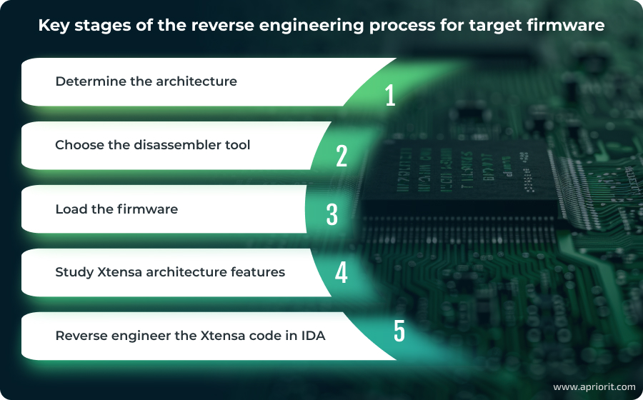
1. Determine the architecture
The first question to ask before reverse engineering IoT devices is how you can know the architecture of the firmware you need to reverse engineer.
The most straightforward way to find out is to read the datasheet for the CPU. But there are situations when all we have is the firmware itself. In this case, we have two options:
1. String search may allow us to find some leftover compilation strings that contain information about the compiler name and architecture.
2. Binary pattern search requires us to know instructions that are often used in different types of microcontroller architectures. We can search the firmware for binary patterns common to a specific architecture and then try to load the firmware into a disassembler that supports such an architecture to validate our guess.
Once we determine the architecture type, we can start choosing the toolset for further reversing. For ESP-32FW.bin, we already knew that this would be the Tensilica Xtensa architecture, so we needed to select the disassembler we would use for our research.
2. Choose the disassembler tool
After researching an appropriate disassembler that could support Xtensa, we ended up with three options: IDA, Ghidra, and Radare.
We decided to try using Ghidra and IDA first because we already have vast experience successfully applying these tools for different reverse engineering projects. And since IDA doesn’t have a decompiler for Xtensa, only a CPU module for the disassembler, we decided to first try working with Ghidra (we used version 10.0).
Ghidra doesn’t support Xtensa by default, so we needed to install the Tensilica Xtensa module for Ghidra first.
The disassembler for Xtensa works, but there are some issues with the decompiler, as you can see in the screenshot below:
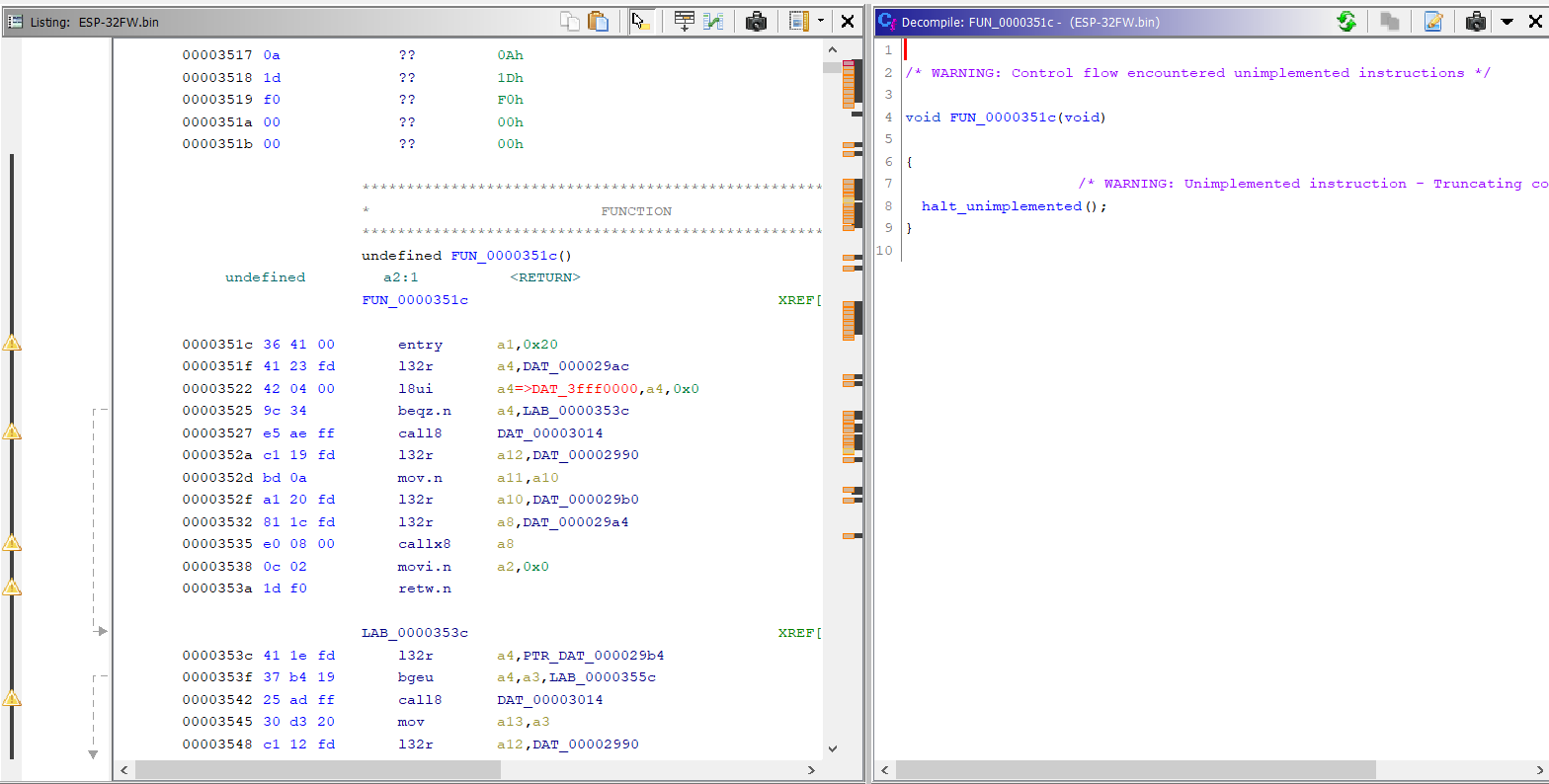
After some time disassembling, we realized that Ghidra’s processor module for Xtensa had trouble determining the instruction length in multiple cases. Therefore, we dropped Ghidra and went to IDA (we used version 7.7).
It was challenging at first to find Xtensa in the list of processor modules, but finally we found it here:
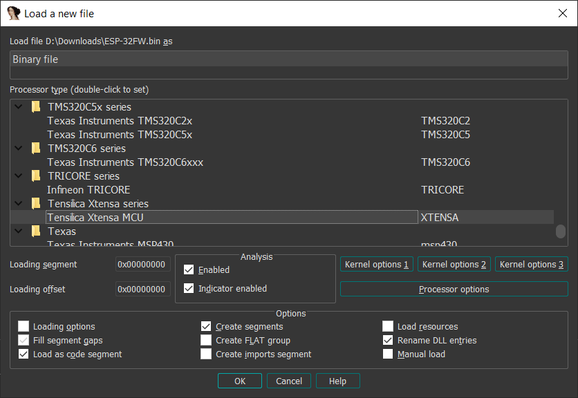
The processor module in IDA appeared to be stable enough, so we decided to stick with IDA.
Read also
9 Best Reverse Engineering Tools for 2023 [Updated]
Discover the top programs for reversing and explore practical examples of using them. Leverage the power of reverse engineering to improve solution’s security, maintain legacy code, and expand software compatibility.
![9 Best Reverse Engineering Tools for 2023 [Updated]](data:image/svg+xml,%3Csvg%20xmlns='http://www.w3.org/2000/svg'%20viewBox='0%200%200%200'%3E%3C/svg%3E)
3. Load the firmware
The first step is to load the firmware to the right image base address so that all of the pointers that are global variables are resolved to valid addresses. To do this, it’s necessary to learn where the code is in the binary.
We start by loading the firmware at the base address 0 and try to mark as much code as possible. To be able to properly mark the code in IDA, we need to learn the typical instruction sequences common to Xtensa firmware. To find out which instructions to use in the function prologs, we took a sample from GitHub: esp8266/Arduino: ESP8266 core for Arduino.
It appears the compiler uses the following instruction: entry a1, XX
This instruction translates into byte sequences such as 36 41 00 / 36 61 00 / 36 81 00 depending on the value of the XX argument.
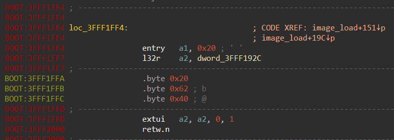
By implementing a simple IDA script to search for such a pattern, it’s possible to mark about 90% of the code:

Once we’ve found the code, it’s time to explore and see whether it looks correct.
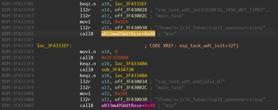
Looking at the screenshot below, it’s obvious that something is wrong. The string resources are referenced properly, but call8 instructions point to strings, not the code. And some of the call8 instructions point to non-existent addresses. Usually this means that the image base is wrong and the firmware must be loaded to some other base address, not 0.
A common way to determine the base address is to:
- Pick a string.
- Use the low part of this string’s address to find the code which references to it.
- Find the difference between the real string address and the address we see in the code. Thus, we can understand how to shift the address of the code to match the current address of the string.
In this case, we found that the base address must be 0x3F3F0000, but even when using it the call8 instructions are still invalid. This could mean that the binary data is segmented and that the code from the flash memory is being mapped to RAM in pieces. Thus, it will be necessary to split the firmware into pieces and load these pieces into IDA in appropriate segments.
We looked at the strings in the firmware and discovered it was indeed segmented:
After additional research, we discovered the ESP IDF framework. Since our target firmware contains some version of this framework, we can try to use its source code to learn about the firmware structure.
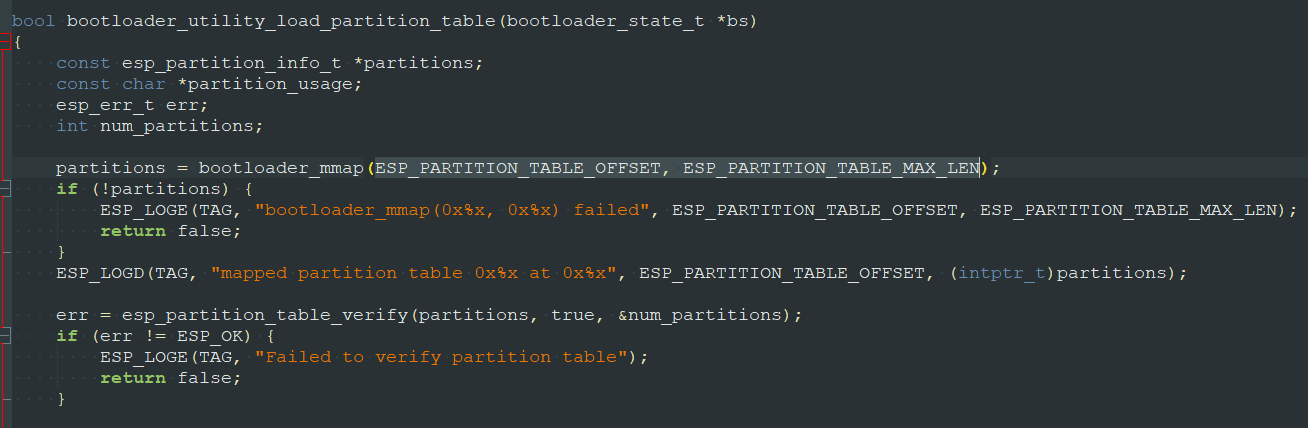
We found an interesting bootloader_utility_load_partition_table() function in the bootloader_utility.c source code file within ESP IDF, which means the firmware must contain a partition table.
To identify the partition table, we continued exploring the source code and finally found the esp_partition_table_verify() function, which is called by the bootloader_utility_load_partition_table() function:
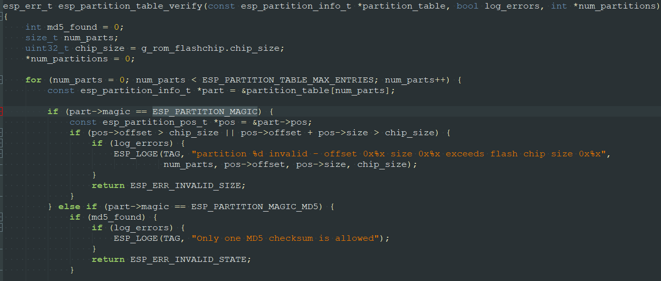
So there must be ESP_PARTITION_MAGIC and ESP_PARTITION_MAGIC_MD5:
#define ESP_PARTITION_MAGIC 0x50AA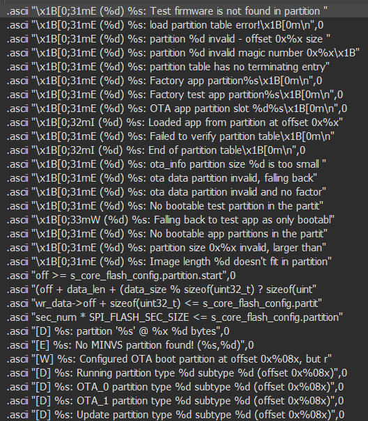
#define ESP_PARTITION_MAGIC_MD5 0xEBEBBinary search for AA 50 gave us good results:
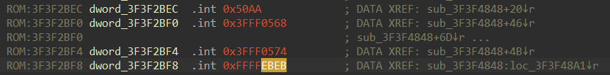
Both ESP_PARTITION_MAGIC and ESP_PARTITION_MAGIC_MD5 can be seen nearby. And most likely sub_3F3F4848 is esp_partition_table_verify().
Since we already know where the esp_partition_table_verify function is, we are able to find the bootloader_utility_load_partition_table function and the ESP_PARTITION_TABLE_OFFSET file offset:
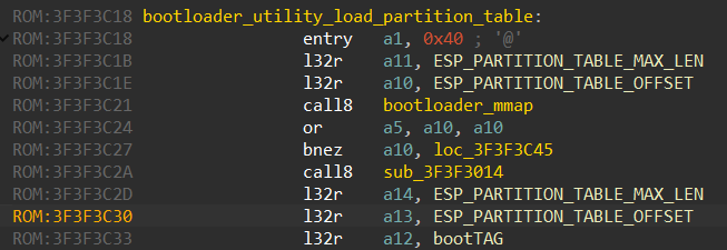
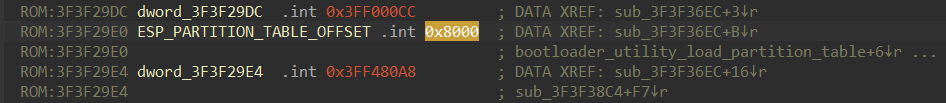
ESP_PARTITION_TABLE_OFFSET is the file offset in the ESP32-FW.bin file. Now we just need to know the structure of the partition table entries. The source code of the ESP IDF framework helps us again:
typedef struct {
    uint32_t offset;
    uint32_t size;
} esp_partition_pos_t;

/* Structure which describes the layout of the partition table entry.
 * See docs/partition_tables.rst for more information about individual fields.
 */
typedef struct {
    uint16_t magic;
    uint8_t  type;
    uint8_t  subtype;
    esp_partition_pos_t pos;
    uint8_t  label[16];
    uint32_t flags;
} esp_partition_info_t;We’ve imported these structures to IDA and applied them to the partition table data:
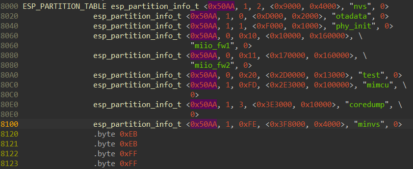
As you can see, esp_partition_pos_t.offset is the file offset for each partition, and we can now split ESP32-FW.bin into the partitions.
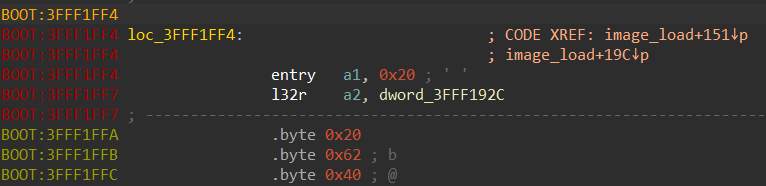
But how can we load each of the partitions to the appropriate address? It appears there’s an image_load() function that is responsible for mapping the firmware partitions onto address space:

And each partition has a header:
typedef struct {
    uint8_t magic;              /*!< Magic word ESP_IMAGE_HEADER_MAGIC */
    uint8_t segment_count;      /*!< Count of memory segments */
    uint8_t spi_mode;           /*!< flash read mode (esp_image_spi_mode_t as uint8_t) */
    uint8_t spi_speed: 4;       /*!< flash frequency (esp_image_spi_freq_t as uint8_t) */
    uint8_t spi_size: 4;        /*!< flash chip size (esp_image_flash_size_t as uint8_t) */
    uint32_t entry_addr;        /*!< Entry address */
    uint8_t wp_pin;            /*!< WP pin when SPI pins set via efuse (read by ROM bootloader,
                                * the IDF bootloader uses software to configure the WP
                                * pin and sets this field to 0xEE=disabled) */
    uint8_t spi_pin_drv[3];     /*!< Drive settings for the SPI flash pins (read by ROM bootloader) */
    esp_chip_id_t chip_id;      /*!< Chip identification number */
    uint8_t min_chip_rev;       /*!< Minimum chip revision supported by image */
    uint8_t reserved[8];       /*!< Reserved bytes in additional header space, currently unused */
    uint8_t hash_appended;      /*!< If 1, a SHA256 digest "simple hash" (of the entire image) is appended after the checksum.
                                 * Included in image length. This digest
                                 * is separate to secure boot and only used for detecting corruption.
                                 * For secure boot signed images, the signature
                                 * is appended after this (and the simple hash is included in the signed data). */
} __attribute__((packed)) esp_image_header_t;Next, each partition is split into segments. And after the header, you can see a structure that is followed by the actual data:
typedef struct {
    uint32_t load_addr;     /*!< Address of segment */
    uint32_t data_len;      /*!< Length of data */
} esp_image_segment_header_t;Here, esp_image_segment_header_t.load_addr is the virtual address for the segment data in the CPU address space.
The segments within the partition look like this:
esp_image_header_t

esp_image_segment_header_t

<segment data>

esp_image_segment_header_t

<segment data>

...Now, having full information about the segments, we can split the partitions into segments and load them to the appropriate addresses in IDA. We can do this extraction work manually or try to automate it via the IDA loader plugin.
Nevertheless, it appears that such a loader is already implemented for Ghidra.
Read also
Using Rust for IoT Development: Everything You Need to Know to Start a Project
Learn how Rust addresses key IoT challenges such as memory safety, performance, and reliability.

4. Study Xtensa architecture features
Now that we have all the segments loaded to the appropriate addresses, we can start the reverse engineering.
But to do it efficiently, we need to learn more about the Xtensa architecture, including:
- Argument order in instructions
- Execution specifics of conditional jumps
- Compiler calling convention
- Stack organization
The first thing to explore is the argument order in instructions. For example: MOV R1, R2. You can find these kinds of instructions in all architectures, yet this may mean either copying R1 to R2 or copying R2 to R1. Thus, it’s crucial to know where the source code is and where the destination register is in the instructions. You can find the Xtensa instruction set description on GitHub.
As for the MOV instruction, in Xtensa, it means that R2 is copied to R1. Thus, the first argument will be the destination in most simple instructions, such as math-related ones. For example, the instruction addi a14, a1, 0x38 would mean that a14 = a1 + 0x38.
But for instructions that store data, it will be the opposite. For example, the instruction s32i.n a5, a1, 0x10 means that the value of a5 must be stored at the address (a1 + 0x10).
The second thing to learn is the way conditional jumps are done. There are two ways to do it:
- Use a dedicated instruction for the comparison operation which sets the flags register and then the conditional jump.
- Use a single instruction that does all those actions at once.
Xtensa does the latter: beqz a10, loc_400E1C54
A single instruction is used to check if a10 equals zero, and then it either jumps to loc_400E1C54 or doesn’t.
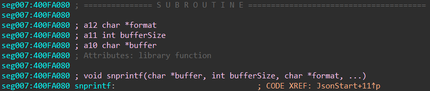
The third step is to examine the calling convention used by the compiler: the way arguments are passed to the function and how the value is returned.
Xtensa passes arguments in quite an unusual way. Arguments are put into registers before the call instruction. But the registers in which they appear within the function are not the same as those they were in before the call:
| Argument index | Register before the call | Register after the call |
| 0 | a10 | a2 |
| 1 | a11 | a3 |
| 2 | a12 | a4 |
| … | … |
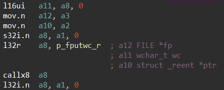
Here’s an example of how to pass arguments to a function on the assembler level:
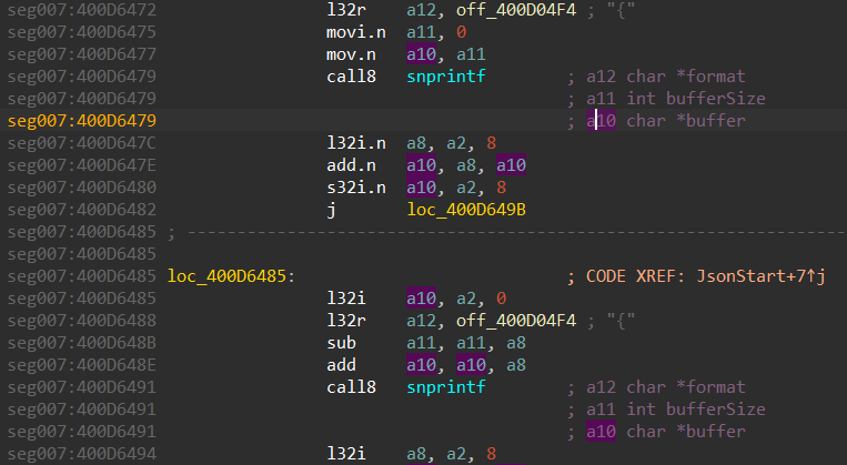
movi.n  a12, 0x14
l32r    a11, off_40080490
mov.n   a10, a1
l32r    a8, memcpy
callx8 a8Here we have three arguments:
- a10 is a destination address
- a11 is a source address
- a12 is the size to copy
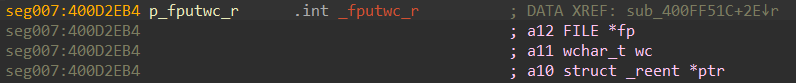
Yet as soon as the code enters the memcpy function, these values are automatically transferred into the a2, a3, and a4 registers respectively.
The same trick is used for returned values. Inside the memcpy function, the value is stored in the a2 register, yet after returning from the function, the value appears in a10.
Here’s what return 0 looks like:
mov.n   a2, 0
retw.nAnd this is what checking the returned value looks like:
call8   jsmi_parse_params
bnez.n a10, loc_400E1B15benz.n checks the value of the a10 register upon returning from the call.
Finally, it’s necessary to learn how the stack is organized.
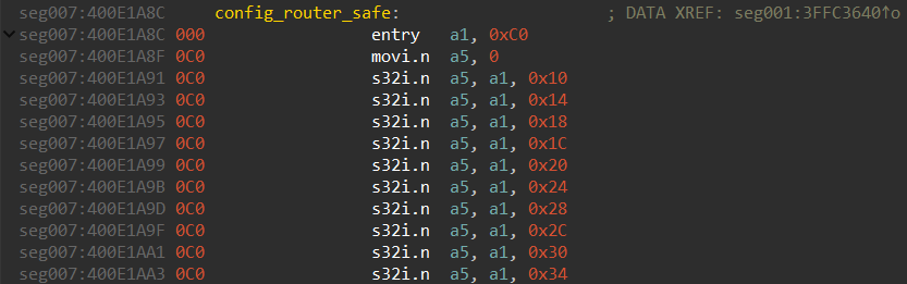
Xtensa uses the a1 register to create the stack frame. Each function starts with the entry instruction: entry a1,0xC0, where 0xC0 is the size of the stack frame, i.e. the amount of stack the function requires for the stack variables.
And often, the functions start with initializing stack variables:
movi.n  a5, 0
s32i.n  a5, a1, 0x10
s32i.n  a5, a1, 0x14
s32i.n  a5, a1, 0x18
s32i.n  a5, a1, 0x1C
s32i.n  a5, a1, 0x20
s32i.n  a5, a1, 0x24
s32i.n  a5, a1, 0x28
s32i.n  a5, a1, 0x2C
s32i.n  a5, a1, 0x30
s32i.n a5, a1, 0x34The zero value from the a5 register is being written in stack variables based on the a1 register.
After gaining all necessary knowledge about the Xtensa architecture, we can finally start reversing its code.
Read also
Reverse Engineering in Cybersecurity: Apriorit’s Best Practices
Discover how reverse engineering empowers security teams to detect weaknesses, analyze malware, and enhance protection strategies.

5. Reverse engineer Xtensa code in IDA
Xtensa isn’t the most popular architecture and doesn’t have a full feature list in contrast to ARM, MIPS, and PowerPC. Therefore, there will be some limitations in the IDA processor module which we need to overcome.
The major limitations of the Xtensa processor module in IDA are:
- No automatic comments for function arguments
- Stack frame is not created automatically
- Some ESP32 functions belong to IROM, so there are calls to hardcoded addresses
- Some Xtensa instructions are not disassembled
Let’s discuss some tricks to overcome these challenges.
5.1. Type system and comments for function arguments
A type system for Xtensa is available starting from IDA 7.7. Having an available type system in IDA is very important, as it makes reversing convenient. In particular, it allows us to import the definitions of C structures and specify the function prototypes used by IDA to put automatic comments near the instructions that transfer the function arguments.
However, if you don’t have a type system, there’s a workaround.
First, let’s look at what functions look like when there’s a type system:
The function prototype is set with the names and types of the arguments so that IDA can use this information to comment the arguments at the call site:
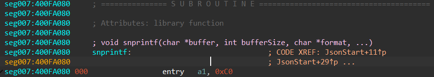
But there will be no such thing for Xtensa. An alternative way is to use the repeatable comments feature in IDA. If we set a repeatable comment at the very beginning of the function, it will be shown at all of the call sites.
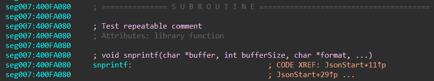
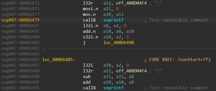
Thus, we can use this feature to define function arguments:
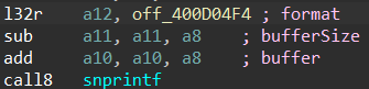
The call site will look like this:
Now, we can select the register name in the comment and IDA will highlight it in the code. Thus, we can easily find an argument value.
5.2. Recover the stack frame
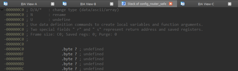
To recover the stack frame, we’ll need to manually specify the stack size and then show IDA where it’s used by pressing K at each instruction that works with the stack.
Let’s explore the config_router_safe function, for example:
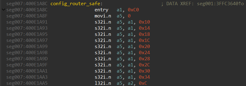
It’s obvious that the stack frame size here is 0xC0. We use this value in the stack settings for the function (Alt+P):
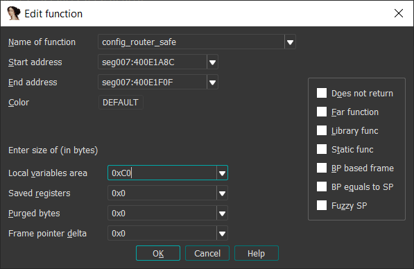
Visually, nothing will happen, but if we go to the stack frame for the function by pressing Ctrl+K, we will notice that stack space is now allocated:
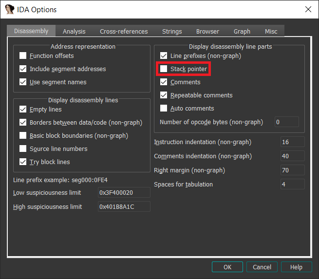
The next thing to do is specify the stack shift using the entry instruction. Before doing that, we suggest enabling the stack pointer visualization as shown in the screenshot below:
Now, the code should look like this:
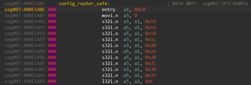
000 is the current stack pointer shift value, and we need to shift it by 0xC0. To do that, we set the cursor at the entry instruction and press Alt+K to see the following window, where we can specify the desired difference between the old and new stack pointer:
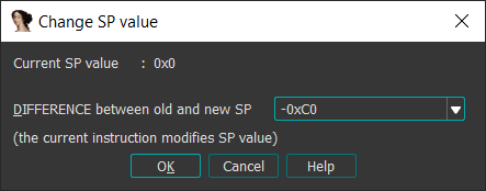
As the result of this operation, the code will look like this:
Now, if we press K at each instruction that works with the a1 register, IDA will create stack variables:
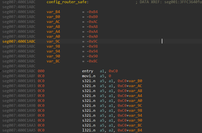
It’s also possible to write an IDA script to automate these actions.
Read also
Discovering and Mitigating Security Vulnerabilities in Routers: A Practical Guide
Ensure reliable and secure work of routers to enhance your embedded software projects by learning the key attack vectors against routers and best practices to secure them.
5.3. Calls to IROM
It’s not uncommon to see calls into some low-level API situated in the IROM part of the CPU and not in the firmware. In such a case, the firmware is just linked with a special linker definitions file containing defined IROM function addresses.
During reversing, IROM function calls look like this:

40058E4C is the address within IROM. But it’s impossible to know which function is called from the firmware. So it’s necessary to inspect the ESP32 toolchain to find the linker definitions.
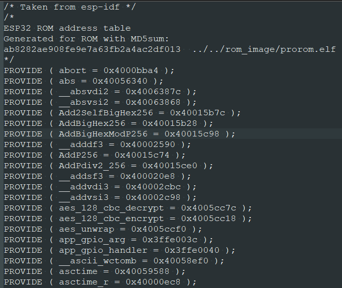
The primary framework for the ESP32 chip is ESP-IDF. It can be used via the Eclipse Plugin or the VS Code extension. The framework relies on legacy IROM addresses, which are available in several formats:
- Raw text in the rom_32.ld stub file
- Base64-encoded values in JSON within esptool
- TOML entries in espflash resources
Below are the contents of the legacy rom_32.ld stub file:
These values can be easily converted into the enum data type:
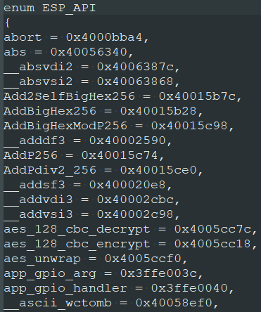
Then, we need to import into IDA so that enum can be applied to the IROM address values:
If we add the repeatable comment near the IROM address, it’ll make everything much easier to read:
Read also
The Evolution of Reverse Engineering: From Manual Reconstruction to Automated Disassembling
Handle security tasks of any complexity efficiently and quickly by fully automating reverse engineering activities. Discover the key techniques, tools, and methods recommended by our cybersecurity researchers.
5.4. Unrecognized instructions
It often happens that the processor module has been implemented for some specific variant of the instruction set. And then manufacturers create new CPUs which have a 99% compatible instruction set of over ten new instructions that nobody expected to have initially. So tools like IDA, Ghidra, and Radare may not be able to disassemble some new instructions.
The proper way to overcome this challenge is to extend the processor module and add support for new instructions. This requires profound knowledge of disassembler APIs, which are not that easy to comprehend.
Let’s discuss a possible workaround for a case when you just want IDA to create the function despite the existence of some unrecognized instruction. Say IDA doesn’t know about the RER instruction and fails to create the function in case it contains RER opcodes:
You can press P as many times you like. Nothing will happen but errors appearing in the console window:
However, it doesn’t mean that IDA can’t create instructions that follow RER instructions. We can skip three bytes of the RER instruction and create the code afterwards:
Next, we select the whole piece of code from entry till retw.n and press P:
After that, IDA will create the function:
Usually, extended instructions that were not recognized by the disassembler don’t make too much difference during reversing. What can cause problems are new instructions that perform actions like a call, a jump, or a load/store, as the code flow is lost and the references to data are missing.
Related project
Auditing the Security of a Connected Vehicle Communication System
Explore how Apriorit’s experts performed a comprehensive audit of a vehicle communication system, identified critical security flaws, and provided improvements that strengthened the client’s automotive cybersecurity posture.

How Apriorit can help with reverse engineering IoT firmware
Reverse engineering firmware isn’t just about digging into code. It’s about protecting your business from hidden risks and achieving long-term product resilience. At Apriorit, we’ve built a team of specialists who combine deep technical knowledge with years of hands-on experience in cybersecurity, embedded development, and cryptography.
When you partner with Apriorit, you will get an expert team that stays on top of:
- Uncovering hidden vulnerabilities. From hardcoded passwords to insecure communication protocols, our engineers identify and explain weaknesses before they can be exploited.
- Analyzing challenging architectures. Our team has experience dissecting non-standard architectures that others can’t handle.
- Providing actionable guidance. Apart from identifying issues, we deliver clear recommendations and remediation strategies tailored to your product’s architecture and business context.
- Supporting complex security initiatives. Whether you’re preparing for certification, strengthening compliance, or planning product modernization, our insights will help you move forward with confidence.
Apriorit has more than two decades of experience partnering with companies across industries to protect their products and intellectual property.
Conclusion
Firmware is the heart of any product. In IoT devices, it can conceal hidden threats like hardcoded credentials, insecure communication protocols, or backdoors. If left unchecked, hackers can exploit these vulnerabilities to compromise not just a single device but entire ecosystems. Identifying them before attackers do is a strategic business move that protects your product, your customers, and your reputation.
Reverse engineering firmware is a complex, highly specialized task. It requires deep knowledge of diverse hardware architectures, security practices, and analysis techniques. That’s why outsourcing this work to an experienced partner is often the most effective approach.
At Apriorit, our reverse engineering team combines expertise in cybersecurity, cryptography, and embedded systems to uncover hidden vulnerabilities and strengthen IoT products. With our in-house specialists and proven methodologies, we help companies secure their firmware against today’s and tomorrow’s threats.
Plan a new IoT project or want to improve an existing one?
Deliver an advanced solution by leveraging Apriorit’s skills and experience in embedded software development and reverse engineering.
What tools are commonly used for IoT firmware analysis?
Popular choices include Binwalk for unpacking images, JTAG/UART for hardware access, and Flashrom or dd for memory extraction.
How can I determine the architecture of firmware?
Utilities like binwalk, file, or readelf can reveal architectural details, and sometimes embedded strings or headers provide additional hints.
Is firmware reverse engineering legal?
Legality depends on the country and intent. It’s often permitted for research, security testing, or interoperability, but it may be restricted under copyright laws, including the Digital Millenium Copyright Act (DMCA) in the US.
What’s the best way to analyze a firmware image?
After image extraction, your engineers can use tools like Ghidra or IDA Pro for disassembly, as well as emulators like QEMU for safe runtime testing.
Why should businesses outsource firmware reverse engineering?
Firmware reverse engineering requires niche expertise and specialized tools. Outsourcing to experienced teams saves time, reduces risk, and helps you find vulnerabilities before attackers exploit them.
How does firmware security affect legal and regulatory compliance?
Strong firmware protection supports compliance with data security requirements (like the GDPR, HIPAA, or NIST guidelines) and helps avoid regulatory penalties.
Can reverse engineering help protect intellectual property (IP)?
Yes. By analyzing firmware, businesses can identify and fix weak spots that could expose proprietary algorithms, encryption keys, or business logic to competitors or attackers.
Have a question?
Ask our expert!
Program Manager