Developers love field-programmable gate arrays (FPGAs) for their reconfigurability. FPGA technology allows you to program certain functionality into the chip and then update it or even change it completely whenever you need. This technology is widely used for developing embedded systems and creating system-on-a-chip (SoC) designs.
The Apriorit team has spent a lot of time studying FPGA technology and has built numerous embedded systems with FPGAs. In this article, we talk about the origins of the FPGA, give a detailed description of an FPGA-specific framework called ISE Design Suite, and look at the main steps you need to take in order to create a VGA driver using FPGA.
Contents:
Understanding FPGA technology
What is a field-programmable gate array (FPGA)? An FPGA is basically an integrated circuit that has an array of programmable logic blocks that can be reconfigured by a developer for nearly any computational purposes.
The first commercial FPGA, the XC2064, was invented by the co-founders of Xilinx Inc. back in 1985. Even today, Xilinx remains one of the leading manufacturers of these circuits.
An FPGA is mainly based on two technologies:
- Programmable Logic Device (PLD) – This is a programmable electronic component with a set of logic gates. Unlike a basic logic gate with a fixed function, a PLD has an undefined function when it’s manufactured, meaning you can reconfigure a PLD the way you need. Moreover, a PLD must be reconfigured before it can be used in a circuit.
- Complex Programmable Logic Device (CPLD) – A CPLD is a PLD built on the idea of personal digital assistants (PDAs), with an interconnection matrix connecting all inputs and outputs. The connection matrix is formed based on the on-chip flash memory to configure macrocells, the main building blocks of CPLDs. Macrocells contain logic that implements disjunctive normal form expressions and specific logical operations.
Over the years, developers have changed the format of FPGAs. Today, this type of integrated circuit has three programmable elements:
- Array of logic blocks
- Routings
- Input/output (I/O) pads
With so many elements that a developer can reprogram for their purposes, an FPGA can perform a large number of vector processing operations simultaneously. Furthermore, an FPGA can even beat a central processing unit (CPU) in processing big data.
When talking about technical capabilities, an FPGA is also pretty similar to an Application-Specific Integrated Circuit (ASIC). Particularly, an FPGA has a high level of energy efficiency and performance, just like an ASIC. But unlike an ASIC, an FPGA can be configured for a specific objective at a much lower production cost and can be easily reconfigured after manufacturing.
Need expert kernel or driver development?
Leverage Apriorit’s deep expertise in low-level programming to build robust and reliable kernel modules and device drivers for your project.
FPGA manufacturers
As we mentioned earlier, Xilinx practically invented the FPGA as a technological solution. Today, the California-based company is one of the two biggest producers of FPGAs and the sure leader in the market.
The second biggest player on the FPGA market is Altera, an innovative company that became part of Intel in 2015. Today, Altera and Intel produce two hybrid circuits, or system-on-a-chip (SoC) FPGAs:
While Xilinx and Altera offer pretty similar solutions, some developers admit that the Altera tools have a more user-friendly and intuitive graphical user interface.
Now let’s talk about the main tasks you can solve with the help of FPGA technology.
FPGA use cases
For a long time, this technology was only used in telecommunications and industrial, military, aerospace, and automotive systems. However, modern FPGA integrated circuits have a much more impressive variety of applications. Thanks to their large logic gate arrays, memory blocks, and fast I/O, FPGAs can perform even the most difficult tasks.
Here are four of the most interesting field-programmable gate array application examples:
- ASIC prototyping and emulation – Also referred to as FPGA prototyping, this is a method of prototyping SoC and ASIC designs on an FPGA. Emulation and prototyping with FPGAs enables fast and accurate SoC system modeling and verification as well as accelerated software and firmware development.
- Cyber security – An FPGA can be effectively used for building network intrusion detection and network intrusion prevention systems. Using an FPGA allows you to improve network monitoring performance. Plus, the reconfigurable nature of an FPGA makes it easier for you to update or completely change the monitoring rules.
- Data center acceleration – When being used as accelerators for data centers, FPGAs can easily be reprogrammed for different accelerator designs. An FPGA helps you process data at high speed and increase the performance of resource-hungry processes and applications for machine learning, edge computing, data mining, and content delivery.
- Artificial Intelligence (AI) – While there’s still a lot of debate going on among researchers, FPGAs show great potential for researching new artificial intelligence algorithms and training AI systems. With an FPGA’s ability to have different blocks performing different tasks, this technology can potentially provide a robust system on a chip. In fact, Microsoft was among the first companies to use an FPGA as part of an AI platform in its Brainwave platform.
In all these use cases, the ability of an FPGA to be programmed and reconfigured for multiple uses is its main benefit. So let’s see how you can configure an FPGA and what tools you can use for it.
Read also
Developing a Simple Display-only Driver for a Graphics Adapter: A Practical Example
Looking to build a Windows driver for graphics adapter from scratch? Explore key techniques and practical insights for developing a display driver, from initial setup to handling user mode interactions in a Windows environment.
Developing an FPGA configuration
Traditionally, to develop an FPGA configuration you would need to use a Hardware Description Language (HDL). While there are many different HDLs, in most cases developers use one of two:
Just as there are plenty of programming languages to choose from, FPGA producers offer numerous frameworks for developing FPGA configurations. For instance, Xilinx provides two FPGA configuration frameworks:
ISE Design Suite can be used for configuring all Virtex-6 and older FPGA families. However, you can also use this framework when working with some of the small and mid-sized Virtex-7 FPGAs.
Vivado Design Suite is a modern framework that doesn’t support older versions of FPGAs. Vivado can only be used with Virtex-7, UltraScale, and newer FPGA families.
As you can see, these frameworks support different generations of FPGA circuits released by Xilinx. The only family that’s supported by both frameworks is Virtex-7. As an alternative, you can use the OpenCL framework.
Let’s look closer at the process of FPGA, using the ISE Design Suite and OpenCL frameworks as examples.
ISE Design Suite
Let’s focus on the main functionality of the ISE Design Suite. When working with ISE, you have a range of project configuration options for a specific circuit. Below, you can see a screenshot of project properties for an FPGA Spartan 6 XC6SLX9 (Figure 1).
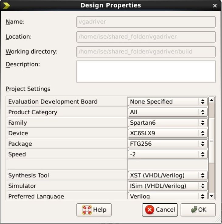
Figure 1. FPGA Spartan 6 XC6SLX9 project properties
There are a number of useful tools in the ISE framework. Let’s look closer at some of these tools and their functionality:
- PlanAhead. This tool is used for visualizing implementation and timing results. PlanAhead makes it easier for you to analyze critical logic and make targeted decisions to improve design performance with floorplanning, constraint modification, and many synthesis and implementation settings.
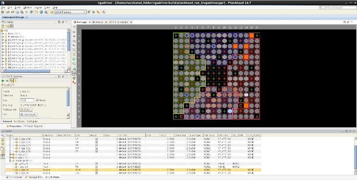
Figure 2. PlanAhead’s Planning I/O ports page
- Design Summary is a tool for collecting configuration statistics. This tool allows quick access to design overview data, reports, and messages.
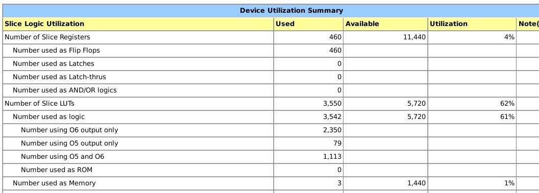
Figure 3. Design Summary
- Core Generator is a tool that provides you with a catalog of architecture-specific intellectual property cores (IP cores), domain-specific IP cores (embedded, connectivity, and DSP), and market-specific IP cores (automotive, consumer, military/aeronautics, communications, broadcast, etc.). The use of the optimized IP cores allows FPGA designers to speed up configuration, saving you days or even months of FPGA design time.
Both ISE and Vivado include a core generator tool called the Clocking Wizard. In Figure 4 below, you can see the Clocking Wizard’s GUI page for generating a module that modifies the frequency of the input clock.
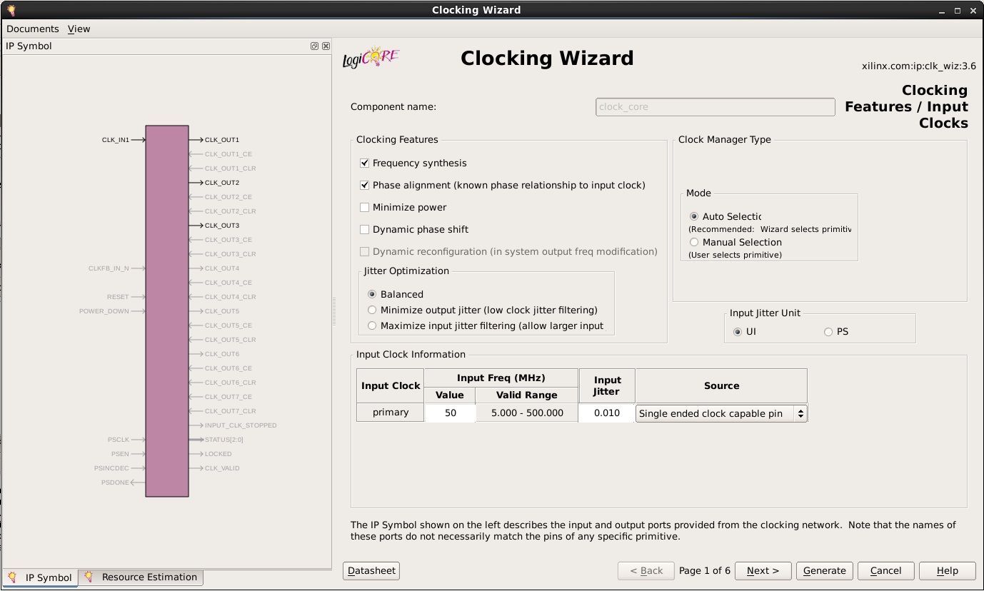
Figure 4. Modifying input clock frequency in the Clocking Wizard
And here’s what the generated module looks like when described in the Verilog language:
// divide clock frequency block
  wire clk_25Mhz;
  wire clk_40Mhz;
  wire sys_clk;
  clock_core clk_divider(
      .i_50Mhz(i_sys_clk),
      .o_25Mhz(clk_25Mhz),
      .o_40Mhz(clk_40Mhz),
      .o_50Mhz(sys_clk)
);- IMPACT is a tool that allows you to perform such functions as Device Configuration and File Generation. The tools have two modes: a console mode (batch mode) and a GUI mode. You can easily work with IMPACT using the user-friendly GUI mode (Figure 5).
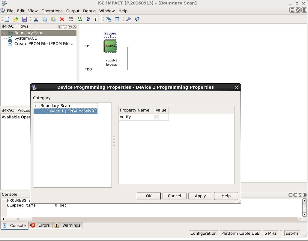
Figure 5. IMPACT GUI mode
However, you can also use the batch mode to send commands to the IMPACT application. Furthermore, when working in console mode you can either send commands one by one or send a set of commands in a .cmd file and program your circuit in one click.
To configure an FPGA, the IMPACT tool uses a .bit file generated by the ISE framework:
- Project Navigator is the primary user interface of the ISE framework. This is where the main configuration development takes place. Project Navigator consists of four main parts:
- A source code editor (Workplace)
- A design hierarchy (Sources)
- A processes tree (Processes)
- An output console (Transcript)
You can use Project Navigator to create a circuit diagram, implement configuration code, manage project files, and collect errors, warnings, and logs.
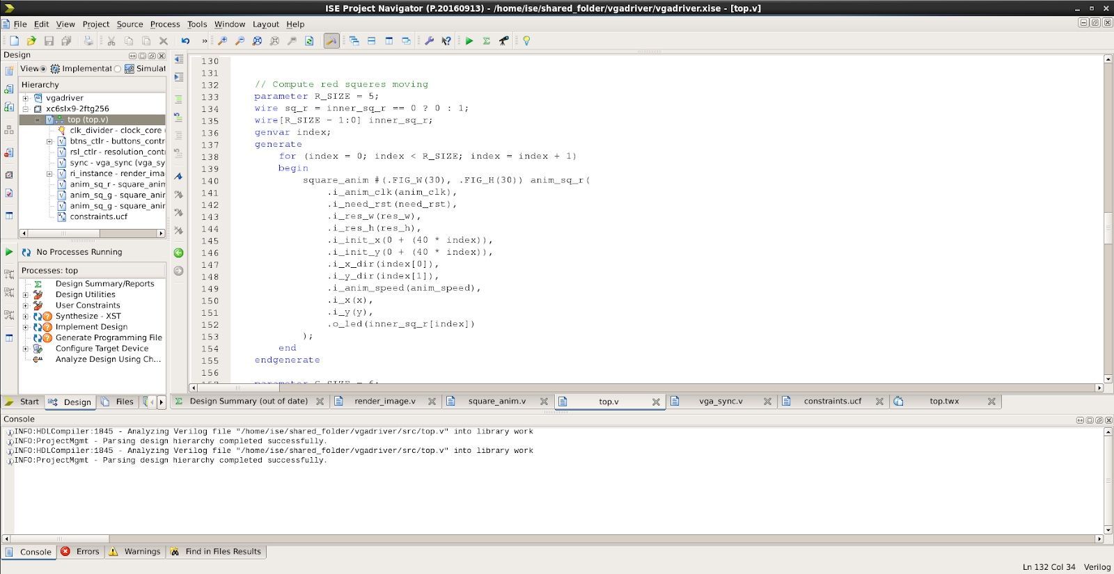
Figure 6. ISE Project Navigator
- ISim is a tool used for system-level testing. It allows you to simulate configuration work and check inner logic without using a real device. In ISim, you can check the counters and the value of register variables and verify logical and timing issues as well as common logic. The simulation can be configured in different ways, for instance by setting clock frequency or constants.
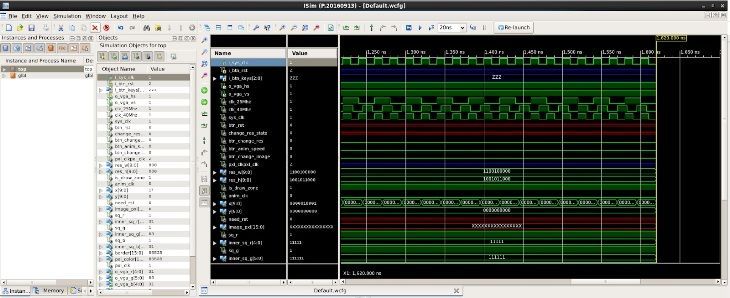
Figure 7. Configuration simulation in ISim
Read also
12 Common Attacks on Embedded Systems and How to Prevent Them
How secure is your embedded system? Explore the most common vulnerabilities in embedded software and strategies to defend against sophisticated attacks from Apriorit experts.
OpenCL framework
The OpenCL framework is a great alternative to ISE Design Suite for developing an FPGA configuration. OpenCL provides a standard interface for parallel computing using task- and data-based parallelism.
When compared to other FPGA configuration frameworks, OpenCL has two main benefits:
- Easier FPGA development. In contrast to the ISE framework, OpenCL includes a C-based language. Therefore, you can use more common high-level programming languages without getting stuck with low-level HDLs.
- Reusable code. In OpenCL, you can significantly extend the life of your code by reusing it for different FPGA generations and families.
Plus, there’s official Intel support for developing FPGA configurations with the help of OpenCL. If you want to learn more about the capabilities and tools provided by this network, check out the official recommendations and real-world examples of using OpenCL for FPGA reconfiguration.
In the next section, we explain how VGA works, focusing on design and implementation of a VGA controller using FPGA.
Developing a VGA driver on FPGA
VGA is a widely used graphics standard for video display controllers. A basic VGA has five main signal pins: three for colors (red, green, and blue), and two more for vertical and horizontal synchronization. Vertical synchronization demarcates a frame (screen), while horizontal synchronization demarcates a line.
An FPGA VGA controller is the perfect use case for testing the capabilities of an FPGA because this standard doesn’t require any complex encoding or high CPU clock speeds. There are different issues you can address when working with these two technologies, from building a simple VGA driver to working on an FPGA open architecture design for a VGA driver.
We’re going to stick to the basics and simply build a VGA driver using FPGA. This driver will perform two simple tasks: display a programmed image on the screen and handle the animation of elements in that image. You can see the result of this work in the video below.
To do this, we’ll use:
Framework: ISE Design Suite
FPGA programming language: Verilog
Circuit: Xilinx Spartan 6 XC6SLX9
Using these tools, we can create an FPGA VGA configuration that works with standard VGA monitors. Depending on the resolution of VGA synchronization timing, the configuration sends VGA monitors the required synchronization signals for displaying the programmed image.
To specify the pin location of monitor signals, you need to create a constraints file. Note that this file should be written specifically for each particular FPGA model.
Here’s a part of the constraints file that connects code variables with the I/O ports of the circuit for our circuit:
// bound VGA pins with code variables
NET "o_vga_hs" LOC = M14;
NET "o_vga_vs" LOC = L13;
NET "o_vga_r[0]" LOC = M11;
NET "o_vga_r[1]" LOC = M12;
NET "o_vga_r[2]" LOC = L12;
NET "o_vga_r[3]" LOC = N14;
NET "o_vga_r[4]" LOC = M13;
NET "o_vga_g[0]" LOC = M9;
NET "o_vga_g[1]" LOC = N9;
NET "o_vga_g[2]" LOC = P9;
NET "o_vga_g[3]" LOC = L10;
NET "o_vga_g[4]" LOC = M10;
NET "o_vga_g[5]" LOC = P11;
NET "o_vga_b[0]" LOC = P7;
NET "o_vga_b[1]" LOC = M7;
NET "o_vga_b[2]" LOC = P8;
NET "o_vga_b[3]" LOC = N8;
NET "o_vga_b[4]" LOC = L7;Our FPGA must also handle the animation of the objects on the screen and compute the exact position for every object at the current moment. To accomplish this, we need to add a specific block to the configuration code base.
Here’s what this block will look like for managing the animation of red squares on the screen:
// Compute red square movements
   parameter R_SIZE = 5;
   wire sq_r = inner_sq_r == 0 ? 0 : 1;
   wire[R_SIZE - 1:0] inner_sq_r;
   genvar index;
   generate
       for (index = 0; index < R_SIZE; index = index + 1)
       begin
           square_anim #(.FIG_W(30), .FIG_H(30)) anim_sq_r(
               .i_anim_clk(anim_clk),
               .i_need_rst(need_rst),
               .i_res_w(res_w),
               .i_res_h(res_h),
               .i_init_x(0 + (40 * index)),
               .i_init_y(0 + (40 * index)),
               .i_x_dir(index[0]),
               .i_y_dir(index[1]),
               .i_anim_speed(anim_speed),
               .i_x(x),
               .i_y(y),
               .o_led(inner_sq_r[index])
           );
       end
endgenerateThis code generates five blocks that call the anim_sq_r module. These blocks run simultaneously with every anim_clk variable tick. The best thing is that even if the count of generated blocks increases, the computation time remains the same.
You can see the result of our experiment with developing a VGA driver using FPGA in the video below.
In this video, we show the processing of two-dimensional objects. The resolution of a basic image is 800×600. By clicking on the buttons on the FPGA circuit, we can change the image resolution, add more objects to the screen, make these objects move across the screen, and even change the animation speed.
Note that this use case has no practical application and is presented for demo purposes only, since our main goal was to check special aspects of image rendering using FPGA resources.
Related project
Developing a Custom Driver Solution for Blocking USB Devices
Discover how we enhanced our client solution’s security with a USB-blocking driver. Apriorit developed a custom driver to block blacklisted USB devices, providing the client with a robust solution to prevent data breaches and unauthorized access to critical systems.
Conclusion
FPGA is a promising technology with great potential for being used in different areas, from developing embedded systems and software to processing big data and training AI algorithms. Today, many IT industry leaders including Intel and Microsoft support this technology and actively use it to improve their inventions.
The main benefit of an FPGA is that it can be reprogrammed multiple times and used for different purposes. Furthermore, an FPGA allows you to configure its blocks for handling different tasks, providing developers with a more robust SoC. Plus, these integrated circuits can be used for accelerating data processing, sometimes even beating the capabilities of traditional CPUs.
Meanwhile, computer vision and image processing remain one of the main use cases for FPGAs. As we’ve shown in our tutorial, you can easily develop a basic VGA driver to handle two-dimensional graphics and simple animations with the help of an FPGA.
Professional assistance is the key to successfully accomplishing even the most challenging tasks. We at Apriorit have a dedicated team of experts in data processing and driver development.
Enhance your system’s performance with custom drivers
Apriorit’s experienced developers will help you build and optimize drivers and kernel modules tailored to your specific hardware and software requirements.


